- English
- French
- German
- Portuguese
- Spanish
- Russian
- Japanese
- Korean
- Arabic
- Greek
- German
- Turkish
- Italian
- Danish
- Romanian
- Indonesian
- Czech
- Afrikaans
- Swedish
- Polish
- Basque
- Catalan
- Esperanto
- Hindi
- Lao
- Albanian
- Amharic
- Armenian
- Azerbaijani
- Belarusian
- Bengali
- Bosnian
- Bulgarian
- Cebuano
- Chichewa
- Corsican
- Croatian
- Dutch
- Estonian
- Filipino
- Finnish
- Frisian
- Galician
- Georgian
- Gujarati
- Haitian
- Hausa
- Hawaiian
- Hebrew
- Hmong
- Hungarian
- Icelandic
- Igbo
- Javanese
- Kannada
- Kazakh
- Khmer
- Kurdish
- Kyrgyz
- Latin
- Latvian
- Lithuanian
- Luxembou..
- Macedonian
- Malagasy
- Malay
- Malayalam
- Maltese
- Maori
- Marathi
- Mongolian
- Burmese
- Nepali
- Norwegian
- Pashto
- Persian
- Punjabi
- Serbian
- Sesotho
- Sinhala
- Slovak
- Slovenian
- Somali
- Samoan
- Scots Gaelic
- Shona
- Sindhi
- Sundanese
- Swahili
- Tajik
- Tamil
- Telugu
- Thai
- Ukrainian
- Urdu
- Uzbek
- Vietnamese
- Welsh
- Xhosa
- Yiddish
- Yoruba
- Zulu
Why Temperature Sensors Matter in Wafer Lithography?
Temperature sensors play a crucial role in wafer lithography, significantly impacting the precision and quality of semiconductor manufacturing. These sensors ensure optimal thermal conditions during the photolithography process, which is essential for creating intricate circuit patterns on silicon wafers. By maintaining accurate temperature control, wafer lithography temperature sensors help prevent thermal expansion or contraction of materials, minimize defects, and enhance overall yield. The ability to monitor and regulate temperature with high accuracy contributes to the production of smaller, more efficient, and more reliable microchips, ultimately driving advancements in various technologies that rely on semiconductor devices.


Wafer lithography is a fundamental process in semiconductor manufacturing, involving the transfer of intricate circuit patterns onto silicon wafers. This procedure requires extreme precision and control over various parameters, with temperature being one of the most critical factors. The photoresist material used in lithography is particularly sensitive to temperature fluctuations, which can affect its viscosity, spreading characteristics, and exposure properties.
During the lithography process, even minute temperature variations can lead to significant issues such as pattern distortion, line width variations, and overlay errors. These problems can compromise the functionality and reliability of the final semiconductor devices. Consequently, maintaining a stable and uniform temperature across the wafer surface is paramount to achieving high-quality results in modern semiconductor manufacturing.
Impact of Temperature Variations on Lithography Outcomes
Temperature fluctuations during wafer lithography can have far-reaching consequences on the quality and performance of semiconductor devices. Some of the key impacts include:
- Pattern Distortion: Thermal expansion or contraction of the wafer can cause misalignment of circuit patterns, leading to defects in the final product.
- Line Width Variations: Temperature changes can affect the dimensions of photoresist features, resulting in inconsistent line widths across the wafer.
- Overlay Errors: Thermal-induced wafer warpage can cause misalignment between different layers of the semiconductor device, compromising its functionality.
- Photoresist Sensitivity Changes: Temperature variations can alter the chemical properties of the photoresist, affecting its sensitivity to light exposure and development processes.
To mitigate these issues, advanced wafer lithography temperature sensors are employed to monitor and control thermal conditions throughout the manufacturing process. These sensors enable precise temperature management, ensuring consistent and high-quality outcomes in semiconductor production.
Advanced Temperature Sensing Technologies in Wafer Lithography
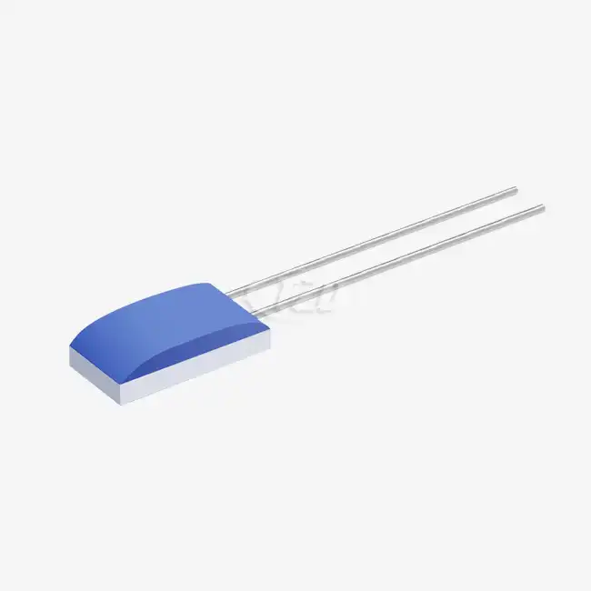
Thin Film Platinum Resistance Thermometers (RTDs)
One of the most widely used temperature sensing technologies in wafer lithography is the thin film platinum resistance thermometer (RTD). These sensors offer exceptional accuracy, stability, and repeatability, making them ideal for the demanding requirements of semiconductor manufacturing. Thin film platinum RTDs, such as those produced by Xi'an Tongzida Technology Co., Ltd., feature a temperature coefficient of 3850 ppm/°C and comply with the IEC60751 standard.
These advanced sensors can cover a wide temperature range from -200°C to +850°C, with an impressive accuracy of ± 0.01 Ω. The long-term stability of these sensors is remarkable, with a drift of ≤ 0.04% after 1000 hours of operation at 500°C. This level of performance ensures consistent and reliable temperature measurements throughout the wafer lithography process.

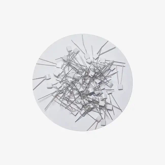
Miniaturization and Integration of Temperature Sensors
As semiconductor manufacturing processes continue to evolve, there is an increasing demand for smaller and more integrated temperature sensing solutions. Modern wafer lithography temperature sensors are available in various compact sizes, ranging from 1.2mm to 4.0mm, allowing for seamless integration into sophisticated lithography equipment.
These miniaturized sensors offer rapid response times, with some models achieving a response time of just 0.05 seconds. This quick reaction capability enables real-time temperature monitoring and control, crucial for maintaining optimal conditions during the fast-paced lithography process. Additionally, these sensors are designed to withstand challenging environmental conditions, with vibration resistance of up to 40g and shock resistance of 100g, ensuring reliable operation in industrial settings.
Multi-point Temperature Monitoring Systems
To achieve comprehensive temperature control across the entire wafer surface, multi-point temperature monitoring systems have been developed. These systems utilize arrays of temperature sensors strategically placed throughout the lithography equipment to provide a detailed thermal profile of the wafer and its surrounding environment.
By employing multiple sensors, manufacturers can detect and address temperature gradients or localized hot spots that may affect the lithography process. This level of granular temperature control enables optimization of thermal management strategies, resulting in improved uniformity and consistency in semiconductor device production.
Optimizing Wafer Lithography Through Precise Temperature Management
Implementing Closed-Loop Temperature Control Systems
To maximize the benefits of advanced wafer lithography temperature sensors, semiconductor manufacturers implement sophisticated closed-loop temperature control systems. These systems continuously monitor temperature data from multiple sensors and make real-time adjustments to maintain optimal thermal conditions throughout the lithography process.
Closed-loop control systems can compensate for various factors that may influence temperature, such as equipment heat generation, environmental fluctuations, and process-induced thermal loads. By dynamically adjusting heating or cooling elements, these systems ensure that the wafer and photoresist materials remain at the ideal temperature for each stage of the lithography process.
Enhancing Yield and Productivity Through Temperature Optimization
The implementation of precise temperature management strategies in wafer lithography can lead to significant improvements in both yield and productivity. By maintaining consistent thermal conditions, manufacturers can:
- Reduce defect rates caused by temperature-related issues
- Improve pattern fidelity and critical dimension control
- Enhance overall process stability and repeatability
- Increase throughput by minimizing temperature-induced delays or rework
These benefits translate into higher-quality semiconductor devices, reduced production costs, and faster time-to-market for new chip designs. As the semiconductor industry continues to push the boundaries of miniaturization and performance, the role of advanced temperature sensing and control technologies becomes increasingly critical in maintaining competitive advantages.
Future Trends in Wafer Lithography Temperature Sensing
As the semiconductor industry progresses towards more advanced manufacturing nodes, the demands on temperature sensing and control technologies continue to grow. Some emerging trends in this field include:
- Integration of AI and machine learning algorithms for predictive temperature control
- Development of ultra-high-resolution temperature mapping techniques
- Advancement in non-invasive temperature measurement methods
- Exploration of novel materials and designs for even more precise and stable temperature sensors
These innovations promise to further enhance the capabilities of wafer lithography temperature sensors, enabling the production of increasingly complex and high-performance semiconductor devices in the future.

Conclusion
Temperature sensors play an indispensable role in wafer lithography, serving as the cornerstone for achieving precision, consistency, and high yield in semiconductor manufacturing. As the industry continues to advance, the importance of accurate temperature control will only grow, driving further innovations in sensing technologies and control strategies. By leveraging cutting-edge temperature management solutions, semiconductor manufacturers can stay at the forefront of technological progress, delivering the next generation of high-performance, reliable, and efficient microchips that power our digital world.
For more information about advanced wafer lithography temperature sensor and other high-precision applications, please contact Xi'an Tongzida Technology Co., Ltd. at sales11@xatzd.com. Our team of experts is ready to assist you in optimizing your semiconductor manufacturing processes through state-of-the-art temperature control technologies.
References
1. Quirk, M., & Serda, J. (2001). Semiconductor Manufacturing Technology. Prentice Hall.
2. Thompson, S. E., & Parthasarathy, S. (2006). Moore's law: the future of Si microelectronics. Materials Today, 9(6), 20-25.
3. Mack, C. A. (2007). Fundamental principles of optical lithography: the science of microfabrication. John Wiley & Sons.
4. Levinson, H. J. (2005). Principles of lithography. SPIE press.
5. Ito, T., & Okazaki, S. (2000). Pushing the limits of lithography. Nature, 406(6799), 1027-1031.


Learn about our latest products and discounts through SMS or email