- English
- French
- German
- Portuguese
- Spanish
- Russian
- Japanese
- Korean
- Arabic
- Greek
- German
- Turkish
- Italian
- Danish
- Romanian
- Indonesian
- Czech
- Afrikaans
- Swedish
- Polish
- Basque
- Catalan
- Esperanto
- Hindi
- Lao
- Albanian
- Amharic
- Armenian
- Azerbaijani
- Belarusian
- Bengali
- Bosnian
- Bulgarian
- Cebuano
- Chichewa
- Corsican
- Croatian
- Dutch
- Estonian
- Filipino
- Finnish
- Frisian
- Galician
- Georgian
- Gujarati
- Haitian
- Hausa
- Hawaiian
- Hebrew
- Hmong
- Hungarian
- Icelandic
- Igbo
- Javanese
- Kannada
- Kazakh
- Khmer
- Kurdish
- Kyrgyz
- Latin
- Latvian
- Lithuanian
- Luxembou..
- Macedonian
- Malagasy
- Malay
- Malayalam
- Maltese
- Maori
- Marathi
- Mongolian
- Burmese
- Nepali
- Norwegian
- Pashto
- Persian
- Punjabi
- Serbian
- Sesotho
- Sinhala
- Slovak
- Slovenian
- Somali
- Samoan
- Scots Gaelic
- Shona
- Sindhi
- Sundanese
- Swahili
- Tajik
- Tamil
- Telugu
- Thai
- Ukrainian
- Urdu
- Uzbek
- Vietnamese
- Welsh
- Xhosa
- Yiddish
- Yoruba
- Zulu
Detailed explanation of Pt100 SMD soldering process: Reflow soldering and wave soldering operation guide
Detailed explanation of Pt100 SMD soldering process: Reflow soldering and wave soldering operation guide
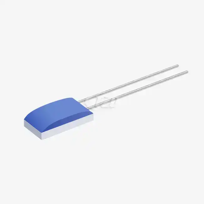
Pt100 SMD thin film platinum resistors support two mainstream soldering processes: reflow soldering and wave soldering. Proper soldering operations can ensure stable sensor performance and secure connections. This article provides a detailed analysis of the operating steps, precautions, and common problem solutions for two welding processes, helping engineers and production personnel efficiently complete welding.

H2: Welding basic information for Pt100-SMD
H3: Core welding parameters
The soldering terminals of Pt100 SMD are made of tin alloy material and are suitable for high-temperature solder paste soldering. The core parameters are as follows:
Recommended solder paste: High temperature solder paste (melting point ≥ 217 ℃);
Welding temperature: 230-240 ℃;
Welding time: peak temperature holding time for reflow soldering is 10-20 seconds, and contact time for wave soldering is 3-5 seconds;
Welding methods: reflow soldering (recommended, suitable for SMT automated production lines), wave soldering (suitable for plug-in assembly).
H3: Preparation before welding
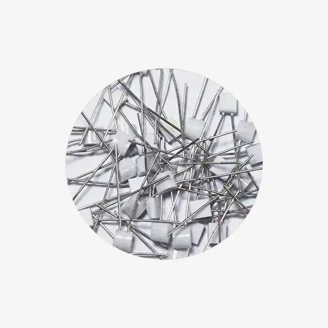
Check the sensor: Confirm that the packaging of Pt100 SMD is intact, without moisture or oxidation, and that the terminals are not deformed or damaged;
Prepare solder paste: Select high-temperature solder paste that meets the requirements, warm it up in advance, and stir it thoroughly and evenly;
Cleaning PCB board: Ensure that the solder pads of the PCB board are free of oil stains, dust, and oxide layers, and perform cleaning treatment if necessary;
Equipment debugging: Debug reflow soldering furnaces or wave soldering equipment to ensure that the temperature curve meets the requirements and the equipment operates normally.

H2: Reflow soldering process operation steps and techniques
H3: Reflow soldering operation steps
Solder Paste Printing: Use a steel mesh to evenly print high-temperature solder paste on the solder pads of the PCB board, with a solder paste thickness controlled between 0.1-0.15mm to ensure uniform printing, no missing prints, and no solder joints;
Mounting sensors: Pt100 SMD is precisely mounted on the solder pads using an SMT machine, ensuring that the sensor terminals are perfectly aligned with the solder pads without any offset or tilt;
Reflow soldering: Send the PCB board with sensors attached to it into a reflow soldering furnace and run it according to the following temperature curve:
Preheating zone: The temperature rises from room temperature to 150-180 ℃, with a heating rate of 2-3 ℃/s, held for 60-90 seconds, and the flux in the solder paste is removed;
Constant temperature zone: Maintain the temperature at 180-200 ℃ for 60-120 seconds to fully activate the flux, clean the solder pads and terminals;
Reflux zone: The temperature rises to 230-240 ℃, and the peak temperature is maintained for 10-20 seconds to ensure complete melting of the solder paste and formation of good solder joints;
Cooling zone: Natural cooling or forced cooling to room temperature, cooling rate ≤ 4 ℃/s, to avoid cracking of solder joints.
Post welding inspection: Check the welding condition of the sensor to ensure that the welding points are full, without defects such as virtual welding, soldering, cold welding, etc. Use a multimeter to measure the resistance value of the sensor and confirm that the performance is normal.
H3: Reflow soldering operation skills
Temperature curve calibration: Regularly calibrate the temperature curve of the reflow soldering furnace to ensure that the actual temperature is consistent with the set temperature and avoid welding defects caused by temperature deviation;
Placement accuracy control: The placement accuracy of SMT surface mount machine needs to be controlled within ± 0.1mm to ensure precise alignment between sensor terminals and solder pads;
Control of solder paste dosage: Excessive solder paste can easily lead to solder continuity, while insufficient solder paste can easily cause virtual soldering. The dosage should be reasonably controlled according to the size of the solder pad;
Cooling method selection: Natural cooling is preferred. If forced cooling is required, the cooling rate should be controlled to avoid temperature drops that may cause damage to the sensor structure.

H2: Operation steps and techniques of wave soldering process
H3: Wave soldering operation steps
Flux coating: evenly apply the flux on the bonding pad of the PCB by spray, foaming or brushing to ensure that the bonding pad is completely covered without omission;
Preheating treatment: Send the PCB board coated with flux into the preheating zone, raise the temperature to 120-150 ℃, and maintain it for 30-60 seconds to remove moisture and volatile substances from the flux and activate it;
Wave soldering: Send the preheated PCB board into the wave soldering slot, allowing the solder pads to come into contact with the solder waves for 3-5 seconds. The soldering temperature is 230-240 ℃, ensuring that the solder paste melts and forms solder joints;
Cooling and cleaning: After soldering, send the PCB board into the cooling area to cool to room temperature, and then clean the residual flux on the surface of the PCB board to avoid corrosion of components;
Post weld inspection: Consistent with reflow soldering inspection standards, check the quality of solder joints and sensor performance to ensure no welding defects.
H3: Wave soldering operation skills
Tin wave height control: The tin wave height needs to be adjusted to just cover the solder pad to avoid excessive contact with the sensor body and damage to the sensor;
Transmission speed control: The transmission speed of the PCB board is controlled between 1-1.5m/min to ensure sufficient welding time and good formation of solder joints;
Selection of soldering flux: Choose soldering flux compatible with high-temperature solder paste to avoid the reaction between soldering flux and solder paste affecting the soldering quality;
Tin bath maintenance: Regularly clean the oxide slag in the tin bath to maintain the purity of the tin solution and avoid defects in solder joints caused by oxide slag.

H2: Common welding problems and solutions
H3: Virtual soldering
Phenomenon: The solder joint is not firm, and the resistance value measured by the multimeter is unstable or infinite;
Reason: Insufficient solder paste usage, low soldering temperature, pad or terminal oxidation, insufficient activation of flux;
Solution: Increase the amount of solder paste, raise the soldering temperature to 230-240 ℃, clean the solder pads and terminals to remove the oxide layer, and replace with more active soldering flux.
H3: Tin plating
Phenomenon: Adjacent solder joints are connected by tin bridges, which may cause short circuits;
Reason: Excessive use of solder paste, misalignment during installation, and high temperature causing solder paste to flow;
Solution: Reduce solder paste usage, adjust mounting accuracy, lower reflow soldering peak temperature or shorten peak holding time.
H3: Cold welding
Phenomenon: The surface of the solder joint is rough, lacks luster, and has poor adhesion;
Reason: Low welding temperature, short welding time, incomplete melting of solder paste;
Solution: Increase the welding temperature, extend the welding time, and check if the melting point of the solder paste meets the requirements.
H3: Sensor performance damage
Phenomenon: Abnormal resistance value of sensor after welding, unable to measure temperature normally;
Reason: Welding temperature is too high, welding time is too long, and the sensor body is in contact with tin waves;
Solution: Strictly control the welding temperature at 230-240 ℃, shorten the welding time, adjust the height of the peak solder wave, and avoid the sensor body from contacting the solder liquid.
FAQ
Q1: Can low-temperature solder paste be used for soldering Pt100-SMD?
A: Not recommended. The melting point of low-temperature solder paste is relatively low (usually ≤ 183 ℃), and the high-temperature resistance of the welded joints is poor. Pt100 SMD may be used in high-temperature environments, and low-temperature solder joints are prone to detachment or failure. It is recommended to use high-temperature solder paste (melting point ≥ 217 ℃).
Q2: Which process is more suitable for Pt100 SMD, reflow soldering or wave soldering?
A: Reflow soldering is more recommended as it is compatible with SMT automated production lines, with high soldering accuracy and efficiency, and can avoid the sensor body from coming into contact with tin solution; Wave soldering is suitable for plug-in assembly or scenarios without SMT equipment, and strict control of the solder wave height is required.
Q3: Is it normal for the resistance value of the sensor to change after welding?
A: A slight change (≤ 0.01 Ω) is a normal phenomenon. If the change exceeds 0.05 Ω, it may be due to excessive welding temperature or improper operation causing damage to the sensor. The welding process needs to be checked and the sensor needs to be replaced.
Q4: How to improve the welding yield during batch welding?
A: Regularly calibrate welding equipment, optimize temperature curves, control mounting accuracy, select high-quality solder paste and flux, strengthen post weld inspections, and establish a comprehensive quality control process.
Q5: How to conduct performance testing on welded sensors?
A: Measure the Ro (0 ℃) resistance of the sensor with a multimeter, which should be within the tolerance range of the corresponding level (A level 100 ± 0.06 Ω, B level 100 ± 0.12 Ω, 2B level 100 ± 0.24 Ω); Test the resistance values at different temperatures to confirm the resistance temperature curve in accordance with DIN EN 60751 standard.
References

Xi'an Tongzida Technology Co., Ltd Pt100 SMD Technical Specification (Version V2.0)
General Specification for SMT Welding Process IPC-A-610H.
The correct soldering process is the key to the excellent performance of Pt100 SMD. Reflow soldering and wave soldering operations must strictly follow technical requirements and control core parameters such as temperature and time. If you encounter problems during the welding process or need more detailed welding process guidance, you can contact Xi'an Tongzida Technology Co., Ltd. Email:sales11@xatzd.comfor professional technical support and customized solutions to make welding work more efficient and reliable!
Author information

Author: Zhao Wei, an electronic manufacturing process engineer. Introduction: With 10 years of SMT soldering process experience, we focus on optimizing soldering processes and solving problems for electronic components. We specialize in providing soldering technical support for precision components such as sensors and chips.

Learn about our latest products and discounts through SMS or email